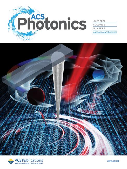
Going beyond the silicon-based electronics is the next major challenge for communications, computing and sensors which will require new functional materials for junctions and transistors. A major barrier for topology-enabled transistors and electronics is the ultimate space-frequency scales that sets the integration density and speed limit for topological junctions, i.e., an interface that occurs between two regions of topological materials with dissimilar band topology. A major limiting factor is our inability to “see” local Dirac fermion conductivity across topological junctions at terahertz-nanometer (THz-nm) limit and our understanding of device physics to efficiently engineering band topology. This paper provides the first evidence of nano-strip heterogeneity in the THz conductivity of Dirac fermions at nanoscales across naturally strained topological junctions. This breakthrough was achieved using a custom-made THz nano-imaging instrument on a Dirac material, ZrTe5. A universal principle of how the junction width depend on the THz electronic conductivity across the junction was revealed. The methodology demonstrated can be extended to characterize a broad range of complex device structures at THz-nm limit, key for developing topological transistors and functional devices.
R. H. J. Kim, C. Huang, Y. Luan, L.-L. Wang, Z. Liu, J.-M. Park, L. Luo, P.M. Lozano, G. Gu, D. Turan, N. T. Yardimci, M. Jarrahi, I. E. Perakis, Z. Fei, Q. Li and J. Wang, “Terahertz Nano-Imaging of Electronic Strip Heterogeneity in a Dirac Semimetal”. ACS Photonics, doi.org/10.1021/acsphotonics.1c00216 (2021) (Cover Article) (2021).

