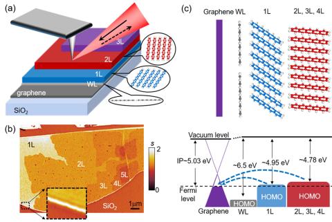
Van der Waals (vdW) heterostructures, which are produced by the precise assemblies of varieties of two-dimensional (2D) materials, have demonstrated many novel properties and functionalities. Here we report a nanoplasmonic study of vdW heterostructures that were produced by depositing ordered molecular layers of pentacene on top of graphene. We find through nano infrared (IR) imaging that surface plasmons formed due to the collective oscillations of Dirac Fermions in graphene are highly sensitive to the adjacent pentacene layers. In particular, the plasmon wavelength declines systematically but nonlinearly with increasing pentacene thickness. Further analysis and density functional theory (DFT) calculations indicate that the observed peculiar thickness dependence is mainly due to the tunneling-type electron transfer from pentacene to graphene. Our work unveils a new method for tailoring graphene plasmons and deepens our understanding of the intriguing nano-optical phenomena due to interlayer couplings in novel vdW heterostructures.
F. Hu, M. Kim, Y. Zhang, Y. Luan, K. M. Ho, Y. Shi, C. Z. Wang*, X. Wang*, Z. Fei*. “Tailor Plasmons in Pentacene/Graphene Heterostructures with Interlayer Electron Transfer”, Nano Letters, Nano Lett. 2019, 19, 6058−6064, DOI: 10.1021/acs.nanolett.9b01945.