Scientific Achievement
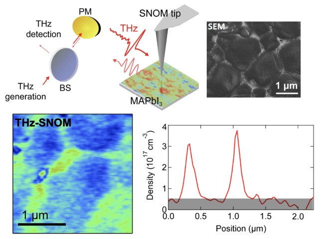
Photo-carrier transport is mapped and visualized at the sub-grain level on a perovskite solar cell material with nanometer spatial resolution and terahertz frequency scales.
Significance and Impact
The dielectric heterogeneity due to charge trapping and degradation in hybrid metal halide perovskite films is mapped at the single grain boundary level. The technique is applicable to various solar cells for their photoconversion performance.
Research Details
- Identified the electron filling at grain boundary traps with terahertz scanning near-field optical microscopy showing an increase of electron density up to ~4 X 1017 cm-3.
- Degradation process of a methylammonium lead halide perovskite MAPbI3 thin film is imaged and identified by tracking the progressive degradation of local nano-defect over a one-week period.
R. H. J. Kim, Z. Liu, C. Huang, J.-M. Park, S. J. Haeuser, Z. Song, Y. Yan, Y. Yao, L. Luo, J. Wang, “Terahertz nano-imaging of perovskite solar cell materials,” ACS Photonics 9, 11, 3550–3556 (2022). http://doi.org/10.1021/acsphotonics.2c00861