Scientific Achievement
A direct relation between the atomic-scale structure of the epitaxial graphene - SiC(0001) interface, which includes silicon (Si) vacancies, and local electronic properties has been established.
Significance and Impact
Epitaxial graphene on silicon carbide (SiC) is a promising platform for graphene-based heterostructures, integrating graphene-based active components into post-silicon micro- and nanoelectronics. The graphene-SiC interface and its complex bonding configurations remain an open challenge.
Research Details
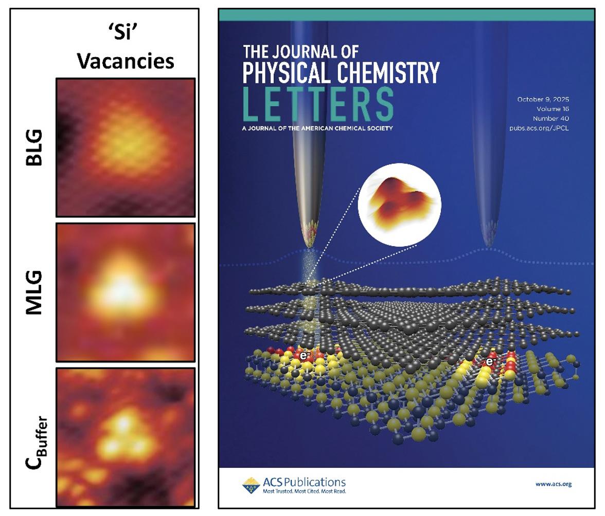
- Controlled synthesis was used to form high-quality graphene with areas of different thicknesses (buffer layer, monolayer and bilayer) on SiC(0001) under ultrahigh vacuum.
- Silicon vacancies at the buried interface below the buffer layer graphene are identified for different graphene thicknesses through the scanning tunneling microscopy and spectroscopy (STM/STS).
- Position and graphene thickness-dependent STM/STS data show locally enhanced charge transfer behavior related to silicon vacancies.
Umamahesh Thupakula, Shen Chen, Yong Han, Michael C. Tringides, and Marek Kolmer, J. Phys. Chem. Lett. 2025, 16, 10487–10498. https://doi.org/10.1021/acs.jpclett.5c02179
This work was performed at Ames National Laboratory.