 Scientific Achievement
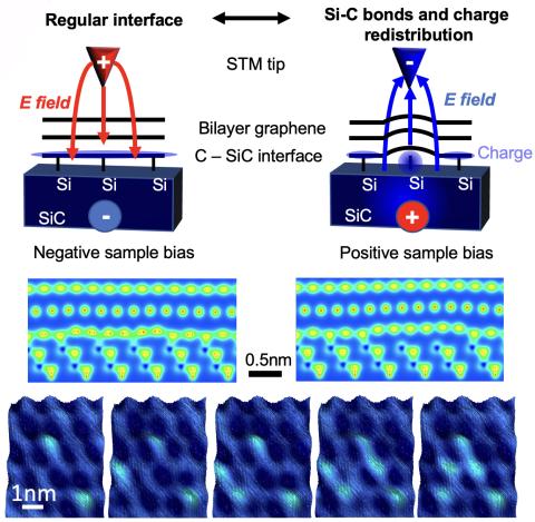
Epitaxial graphene patterning platform is developed by using the scanning tunneling microscope (STM). A local electric field controls the covalent C-Si bonds at the buried graphene – SiC interface, allowing their reversible breaking and formation.
Significance and Impact
Directly creating arbitrarily large lateral unit cells with graphene layers may allow for their controllable quantum properties.
Research Details
- Synthesizing high-quality epitaxial monolayer and bilayer graphene heterostructures enables the electric field manipulation platform via systematic control of tip-sample bias voltage in STM experiments.
- Large-scale density theory calculations model the exact atomistic picture of the C-Si covalent bonds redistribution during STM manipulation events.
- Typical STM atomic manipulations are performed on surface atoms or adsorbates. The proposed platform consists of an atomically defined yet buried interface (left, top four panels). Thus, the patterns (left, bottom panels) are naturally protected by the top graphene layers and can serve as a tunable template for two-dimensional (2-d) material synthesis.
“Atomic-scale manipulation of buried graphene–silicon carbide interface by local electric field”, M. Kolmer, J. Hall, S. Chen, S. Roberts, Z. Fei, Y. Han, M.C. Tringides, Communications Physics 7, 16 (2024), https://doi.org/10.1038/s42005-023-01515-3